Semiconductor
The World's Largest Chip: Why Cerebras Built It, and How
July 13, 2026 · 47 reads
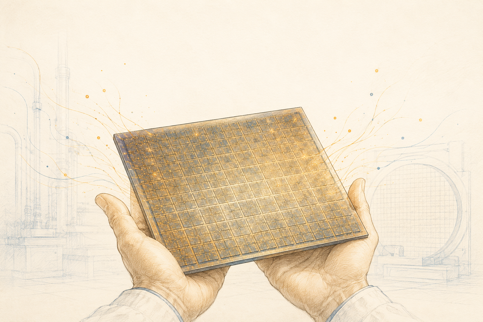
The first time I ran into the Cerebras WSE-3, I had to look twice. It’s a single chip about the size of a dinner plate: 21.5 cm on a side, comfortably bigger than my face, and it holds the record for the largest chip ever made. Why would anyone build a chip this big? How do you even manufacture something that large without it falling apart? And what actually breaks when you try?
The why, the how, and the what-breaks: those three questions are what this post is about.
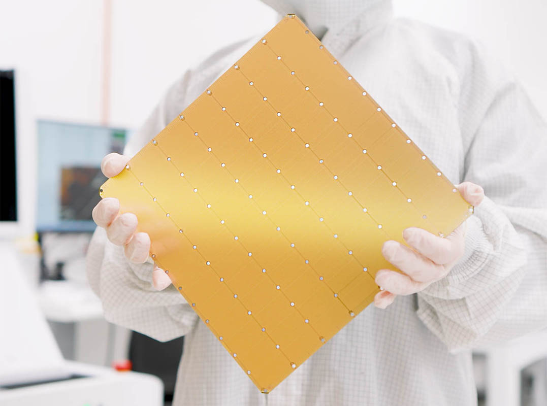
The Cerebras WSE-3, one wafer, uncut, held like a serving tray.
Part One: The chip itself
Cerebras’s flagship is the WSE-3 (Wafer-Scale Engine 3), and the simplest way to describe it is a chip that never got cut up. A normal fab prints dozens of identical dies onto a 12-inch wafer and then slices them apart into separate chips. Cerebras does the opposite: it leaves the wafer whole and wires the dies together, turning the scribe lines (the thin dead zones between dies) into data highways. Every row and column gets connected, and the whole wafer becomes one continuous 2D mesh: 84 dies, roughly 10,000 cores each, with every core split half-and-half between SRAM (48 KB) and logic.
That “don’t cut, connect” move is the genuinely novel part. The patent lists five ways to pull it off; the animation below walks through the first.
If that didn’t quite land, it helps to back up to how ordinary chip-printing works. The round silicon disc is the wafer. Each finished block of circuitry on it is a die. During lithography, a scanner projects the circuit pattern off a photomask onto the wafer, lining the mask up over one die at a time.
Cerebras’s trick is almost cheeky: nudge that photomask a hair along the X or Y axis (an offset exposure) so the pattern straddles the gap and prints wiring between two neighboring dies. Nothing about the lithography process changes; only where the mask lands. And that’s the whole point: talking across dies this way is far cheaper than stitching separate chips together on a board.
The second break from convention is where the memory lives. A GPU keeps most of its data in HBM stacks parked off to the side of the processor, reached across a silicon interposer and several layers of solder. The WSE-3 keeps compute and memory on the same die, joined by plain copper, and that single decision sends bandwidth through the roof: roughly 21,000 TB/s of main-memory bandwidth, against 8 TB/s on a B200 and 3.35 TB/s on an H100. Not a little more. Thousands of times more.
Part Two: Why bandwidth is the whole game
Why is more bandwidth so important in AI inference? it does solve one very specific, very expensive problem: it stops the compute cores from sitting idle, waiting for data. When a large model generates text, producing each token means reading a mountain of weights, and the bottleneck usually isn’t “the math is too slow.” It’s “the data can’t arrive fast enough.” That’s the memory wall, and it’s the thing everyone in this business is fighting.
The cleanest way to reason about it is the roofline model, which ties together three numbers: how fast you can compute (FLOP/s), how fast you can move data (bandwidth), and arithmetic intensity (how many FLOPs you do per byte you move). Your real-world performance is whichever ceiling you hit first: raw compute, or bandwidth times intensity.
Achievable performance = min( peak FLOPs, bandwidth × arithmetic intensity )
The roofline: the flat compute ceiling, the bandwidth ramp, and the ridge between them.
Everything to the left of that ridge is memory-bound: the cores idle, starved for data. And here’s the kicker: nearly all AI inference lives on the left side. To generate token N, the chip has to read the entire model’s weights plus the KV cache just to compute that one token: trivial math, enormous data movement. In some cases you’re using well under one percent of the chip’s peak compute. Which is exactly why Groq’s LPU, Google’s inference TPUs, and the WSE-3 are all obsessed with the same thing: feeding the cores faster.
Part Three: Had anyone even tried this?
The dream of one giant chip isn’t new. Someone chased it decades ago, and it’s a genuinely strange story.
Back in the 1980s, Gene Amdahl, the lead architect behind IBM’s System mainframes, set out to build a near-wafer-scale “super chip” that kept most of its data on the processor itself. His company, Trilogy, raised a then-record $230 million. Then everything that could go wrong did: a storm knocked out the fab’s air conditioning and let dust into the cleanroom, a senior executive died of a brain tumor, and Amdahl himself got tangled up in a car accident and a lawsuit. The packaging, cooling, and testing of the era weren’t close to ready either. The whole thing collapsed.
Decades later, the failed dream finally met an era that could support it, but the engineering was still brutal. Cerebras’s own IPO prospectus put it about as dramatically as a legal filing can:
Nobody knew how to yield a chip 58 times larger than the leading GPU.
Nobody knew how to deliver power to a chip the size of a dinner plate without melting the motherboard.
Nobody knew how to package such a big chip without cracking it.
Nobody knew how to cool a chip of this size, with air or water, without the coolant getting warm before it reached the other side.
Nobody knew, and we didn’t know either.
(Cerebras S-1 prospectus)
Four walls, then. Let’s take them one at a time.
Wall One: Yield, a chip 58× bigger than a GPU
Yield is just the fraction of chips that come off the line actually working, and the intuition for why it’s a nightmare here is easy to build:
Think of Minesweeper. The bigger the board, the more mines it hides. A tiny 3×3 grid might have none, and you clear it without thinking. Blow the board up to fill your screen and mines are everywhere. Chips are the same. The bigger the wafer, the more defects: a speck of dust, a chemical non-uniformity, a lithography slip. Normally you just toss the bad dies and sell the good ones. But a chip that’s one giant die fails the instant a single spot goes bad. Out of ten thousand wafers, not one would come out flawless.
Cerebras beat this with two moves. First, it makes each core absurdly small, just 0.05 mm², so a single defect only takes out a sliver of the chip. (On a GPU, one bad spot can force you to disable a whole 6.2 mm² unit, over a hundred times larger.) Second, it holds about 7% of the cores in reserve; when testing turns up dead ones, the on-chip network quietly reroutes around them and swaps in the spares. Net result: 93% of cores active, and yield close to 100%.
Tiny cores plus redundant routing: how a “zero-yield” chip becomes shippable.
Wall Two: Power, without melting the board
Cerebras built its chip a custom home, the CS-3 server, and it draws 25 kW, on the order of 25,000 amps. Put it in household terms: it’s the current of every main breaker in about 625 homes, all maxed out at once, feeding a single server.
Current that big gets delivered the usual way, by stepping the voltage down in stages: high-voltage/low-current far from the chip, dropping to around 1 V right at the die. But the flat, sideways layout most boards use has two nasty failure modes once you’re pushing 25,000 A.
Problem one: voltage drop. From Vdrop = I × R, at 25,000 A even a hundred-thousandth of an ohm produces a 0.25 V drop, and against a 1 V core, that’s a 25% loss before the power even arrives.
Problem two: heat. From P = I × V, that same 0.25 V becomes 0.25 × 25,000 = 6,250 watts of heat dumped into one small spot.
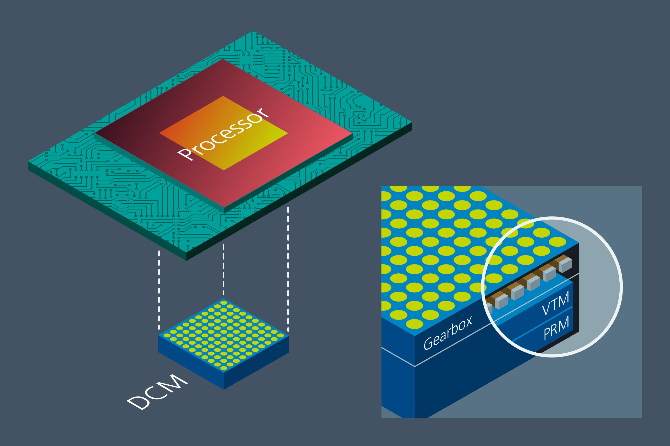
Cerebras’s answer, built on Vicor’s hardware, is to stop sending the current sideways at all. In place of the lateral layout it uses vertical power delivery: the final voltage converters sit directly underneath the processor, so the enormous current travels the shortest path it possibly can.
Vertical delivery: converters tucked right under the chip, path cut shorter.
Wall Three: Packaging and cooling
A 25 kW machine has a serious heat problem to begin with, and the WSE-3’s sheer size adds a twist.
Almost everything expands when it heats up. A small GPU die barely budges. Scale the area up, though, and even a mild temperature swing produces a very real amount of movement, and inside a package, a few tens of microns is enough to tear micron-scale solder joints apart. Worse, heat the wafer unevenly and it expands unevenly, which means mechanical stress and warping.
The real villain is the CTE mismatch: the fact that different materials expand at different rates. Silicon barely moves (~2–3 ppm/°C); copper and the PCB move a lot (~15–17 ppm/°C). Heat both by 60 °C and the difference in expansion reaches about 160 μm, roughly the width of a human hair, more than enough to rip solder joints and pry a package open. A 3 cm GPU die, over the same temperature rise, differs by only a few microns, which the solder’s own springiness can soak up.
That pushed Cerebras into a genuinely unusual package, the heart of the CS-3, which they call the Engine Block: a cold plate on top, the chip in the middle, the PCB underneath, and special connection layers in between. The guiding idea is easy to state and hard to build: let the vertical direction do the real work (carry heat or current straight through) while letting the horizontal direction slide freely to absorb all that mismatched expansion.
Take the sliding thermal layer as an example. It’s indium on the cold-plate side (which conducts heat well) pressed against an ultra-thin PTFE (Teflon) film on the wafer side (which is slippery). The two are pressed together but never soldered, so they can slide against each other. Between the wafer and the PCB sits a silicone sheet studded with conductive particles that touch vertically to carry current while still sliding horizontally. A normal GPU just solders its die straight to copper, and it’s small enough that the solder’s elasticity handles the rest.
The catch: a lot of things are custom
Add it all up and the list of things Cerebras had to reinvent is long: the chip’s size, scribe-lines-turned-wiring, high yield on a monster die, tiny cores, on-die SRAM, the solder-free Engine Block, vertical power delivery. And it pays off: in published benchmarks, the WSE-3 puts out tokens per second tens of times faster than a GPU.
But every one of those wins comes with the same string attached: it’s all bespoke. The cross-die process is an exclusive partnership with TSMC (“not easily portable to another foundry,” as the prospectus admits), so if TSMC’s capacity gets tight, there’s no plan B. The vertical power comes from Vicor, which has already said it’s running at capacity. And the CS-3 runs so hot per square inch that it needs colder inlet water than a standard machine room provides: bigger pumps, fatter pipes, higher-flow fittings, none of it off-the-shelf.
It all points the same way. The custom route is exactly what makes the WSE-3 possible, and exactly what caps how fast Cerebras can grow: single-source suppliers at every critical node, no fit into a commodity data center, power and cooling both built to order. Whether all of that can turn into a dependable supply chain is, in the end, the question that decides how steady the company’s path turns out to be.