Baking a Model Into Metal: How Taalas Beats the HBM Bottleneck
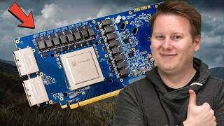
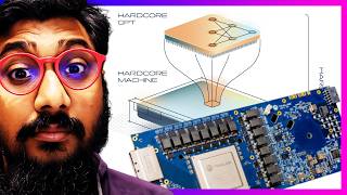
Every GPU serving a large language model pays a hidden tax: it has to keep pulling the model's weights out of HBM memory and shuttling them to the compute cores before it can do any math. Taalas' approach is to eliminate that trip entirely. Its first chip, the HC1, is built on TSMC's 6nm process as an 815 mm^2 die packing 53 billion transistors, and instead of loading Llama 3.1 8B's weights from external memory, the weights and dataflow are etched directly into the chip's own metal layers [2]. The result, per Taalas' own benchmark, is roughly 17,000 tokens per second for a single user on that model [2]- a number multiple outlets put at somewhere between 48x and 73x faster than general-purpose GPUs on the same workload, with SiliconANGLE citing a claim of 73x versus an Nvidia H200 at one-tenth the power, and the Register citing 48x versus GPUs and 8.5x versus Cerebras accelerators [1][3].
The trick that makes this commercially viable rather than a one-off curiosity is how little of the chip actually has to change to target a new model. Of a chip's 100-plus metal/mask layers, Taalas says only about two upper layers encode the model-specific weights and matrix dimensions, so a full re-spin for a new model takes roughly two months instead of the industry's typical one-to-two-year design cycle [2][4]. That is the whole bet: give up general-purpose programmability, and in exchange get GPU-beating speed, cost, and power for whichever model you're willing to hardwire in. The obvious catch, which AMD is buying along with the upside, is that these chips can't be reprogrammed like software - a meaningfully different model means a new tape-out, not a firmware update [1].