Huawei's Tau Scaling Law and LogicFolding chip design
TECH

Huawei's Tau Scaling Law and LogicFolding chip design

33+
Signals

Strategic Overview

  • 01.
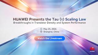
    On May 25, 2026, HiSilicon president He Tingbo used his ISCAS 2026 keynote in Shanghai to propose the Tau (τ) Scaling Law as a successor to Moore's Law, shifting the optimization target from transistor geometry to resistance-capacitance signal delay across picosecond-to-second scales.
  • 02.
    Paired with the announcement is LogicFolding, an architecture that vertically stacks digital, analog, and memory layers at the design stage to push transistor density from 155 to 238 MTr/mm² (+53.5%) on the same process node.
  • 03.
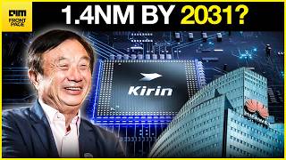
    Huawei says it has already designed and mass-produced 381 chips under the τ framework over six years, and projects 1.4 nm-equivalent density for its high-end chips by 2031 despite being cut off from EUV lithography.
  • 04.
    The Kirin chips launching in Fall 2026 will be the first commercial silicon to adopt LogicFolding, with a CPU performance-core frequency roadmap of 3.1 GHz (2026) → 3.39 GHz (2027) → 3.71 GHz (2028) → >4 GHz (2029) and a claimed 41% improvement in performance-core energy efficiency.
  • 05.
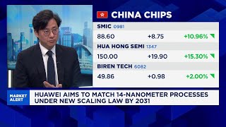
    Markets read the announcement as material: SMIC rose 18%, Hua Hong Semiconductor hit its 20% daily limit, and the Shanghai Star 50 touched record highs the same day.

Deep Analysis

Why Tau changes the scoreboard, not just the score

The Tau Scaling Law's strategic move is redefining what "better" means in silicon. For sixty years the industry has chased Moore's Law — more transistors per mm² as features shrink. Huawei's τ proposal pivots the optimization target to the resistance-capacitance time constant of signals propagating across a chip, measured across picosecond-to-second scales, and treats geometry as just one of many levers to pull on it [1][7]. If the metric of progress is signal delay rather than transistor pitch, then 3D stacking, novel materials, and architectural tricks all become first-class scaling techniques rather than workarounds for a missing EUV machine. Futurum's Brendan Burke calls τ "the most theoretically coherent post-Moore framing yet," precisely because it gives a unified yardstick for benefits that Moore's Law has no language to compare [4]. The political subtext is sharper: a firm cut off from EUV cannot win a transistor-shrink race, but it can credibly try to win a time-domain race — and the sell-side has started reading the move as the practical end of Moore's Law for Chinese chipmakers.

What tau actually is: τ = R×C, the time constant of a wire under load, in plain terms how long a signal takes to settle from one logic state to the next. Shrink the transistor and you do shorten one part of that delay, but in modern SoCs the interconnect (wire) contribution dominates. Optimizing τ directly forces designers to think about wire length, capacitance, and routing congestion as first-order metrics — places where EUV gives you little advantage anyway.
Folding gates, not chips: the technical line that matters

LogicFolding's load-bearing technical claim is that it stacks at a finer granularity than anything in mass production. The hardware community framed the hierarchy cleanly on Reddit, distinguishing three stacking levels by what gets bonded. TSMC's CoWoS stacks at the chip level — an interposer wires complete, independently functional dies together. AMD's 3D V-Cache stacks at the block level — a finished SRAM die is bonded on top of a finished CCD. Huawei's LogicFolding, as described, stacks at the logic-gate level — EDA tools partition the gates of a single functional block across two dies so that neither die is functional on its own. That is what lets Huawei report transistor density jumping from 155 to 238 MTr/mm² (+53.5%) on the same underlying process node and claim the resulting Kirin block rivals TSMC's 3nm density [8][9].

The architecture also targets the time-domain prize that gives Tau its name: by physically folding logic into vertical stacks, Huawei says it shortens critical-path wiring, the single biggest contributor to RC delay in modern SoCs [1]. Hardware-community discussion described it as far more fine-grained than prior industry stacking work, with chip designers viewing the resulting stack as one part for layout purposes. The gate-level granularity is the load-bearing engineering bet: it's why Huawei argues this is not just better packaging but a different design paradigm.

Marketing rebrand or real physics? The skeptics' case

The contrarian read is that Huawei changed the ruler because it didn't like the measurement. Omdia's Manoj Sukumaran is the bluntest: "The '14 angstrom equivalent by 2031' is not a process-node claim. Huawei is stuck on 7nm," arguing the headline number is hybrid bonding and packaging dressed as a node, and that each added stacking layer delivers diminishing returns [3]. Independent analyst Ian Cutress echoes the framing, saying Huawei is "arguing apples and oranges" by comparing specs across unrelated chips [10].

An engineering objection the press releases skip surfaced in hardware-community discussion: stacking heat-generating logic layers on top of each other concentrates thermal density, raising throttling risk that gets worse with every fold. The skeptic synthesis is that density-equivalent is not the same as a true process node, the comparison set is hand-picked, and the thermal and yield costs of fine-grained logic-gate stacking are unproven at consumer-product volume — all caveats the equity reaction conspicuously ignored, with SMIC closing +18% and Hua Hong Semiconductor hitting its 20% daily limit the same day [5].

The 381-chip dress rehearsal

The most under-discussed line in the keynote is the claim that Huawei has already designed and mass-produced 381 chips using the τ framework over the past six years before going public [1][2]. If true, the ISCAS announcement is less a moonshot and more the public reveal of a stealth program with shipped silicon as its evidence base — a fundamentally different risk profile than a research-paper claim. The empirical proof point arrives on a known clock: the Kirin chips launching in Fall 2026 will be the first commercial parts to use LogicFolding.

Huawei has published a year-by-year CPU performance-core frequency roadmap of 3.1 GHz (2026) → 3.39 GHz (2027) → 3.71 GHz (2028) → >4 GHz (2029) with a 41% performance-core energy-efficiency gain in the first generation [2][8]. Those are falsifiable. The things to watch in Q4 2026 are independent die-shot analysis of the Kirin part, third-party density measurements against the claimed 238 MTr/mm², and thermal behavior under sustained load — the three places skeptics like Sukumaran say the architecture should crack [3]. If the first generation hits, the 2027 part with the further frequency step becomes the next checkpoint; if even one generation undershoots, the diminishing-returns critique gains weight quickly.

Whose moat just got narrower: TSMC, ASML, and the global stack

The market reaction told the geopolitical story in one trading session. SMIC closed up 18%, Hua Hong Semiconductor hit the 20% daily limit, and the Shanghai Star 50 touched record highs — investors pricing in a credible domestic Chinese path to leading-edge equivalence without ASML [5]. The implications fan out in three directions. First, ASML's leverage as the sole-supplier chokepoint weakens at the margin if design-stage stacking can substitute for several nodes of geometric scaling — even Omdia's skeptics concede Huawei is "in the right direction" [3].

Second, TSMC's process-leadership moat — 1.4nm mass production by 2028 versus Huawei's density-equivalent 2031 — remains intact in absolute terms but loses its monopoly framing, because Huawei now has, in Omdia's Lian Jye Su's words, "an alternative path forward" [6]. Third, the world inches closer to a bifurcated semiconductor stack: a TSMC/Intel/ASML EUV ecosystem and a Huawei/SMIC stacking-and-design ecosystem, each optimizing for a different metric. Sell-side commentary on X read the announcement as a direct read-through to TSMC's existing CoWoS-L and SoIC advanced-packaging programs — the bull case for incumbents now leans more heavily on those packaging roadmaps than on the EUV moat alone.

Historical Context

2019
U.S. export controls landed on Huawei, eventually cutting it off from ASML's EUV lithography systems and from leading-edge foundry services — the constraint that drives the τ and LogicFolding strategy.
2023-08
The Mate 60 Pro launch with a 7nm Kirin chip produced by SMIC surprised the industry and signaled Huawei could route around sanctions on advanced fabrication.
2026-05-25
Tau (τ) Scaling Law and LogicFolding unveiled at IEEE ISCAS 2026 in Shanghai, with a Kirin Fall 2026 product debut and a 1.4nm-equivalent density target by 2031.
2028
TSMC targets mass production of true 1.4nm process chips by 2028, roughly three years ahead of Huawei's density-equivalent claim and the implicit benchmark for whether LogicFolding closes the gap.

Power Map

Key Players
Subject

Huawei's Tau Scaling Law and LogicFolding chip design

HE

He Tingbo

Huawei Board Member and President of HiSilicon; delivered the ISCAS 2026 keynote unveiling τ Scaling and LogicFolding.

HU

Huawei / HiSilicon

Author of the Tau Scaling Law and LogicFolding architecture; will debut both in Fall 2026 Kirin SoCs after six years of internal validation across 381 chips.

SM

SMIC

Chinese foundry partner producing Huawei Kirin chips on a 7nm-class node; shares rose 18% on announcement day.

HU

Hua Hong Semiconductor

Chinese foundry; shares surged the full 20% daily limit on the news.

TS

TSMC

Process-leadership benchmark; targets mass production of true 1.4nm chips by 2028, roughly three years ahead of Huawei's density-equivalent 2031 goal.

AS

ASML

Dutch supplier of EUV lithography systems blocked from selling to China under US-led sanctions — the constraint Huawei's design-stage stacking attempts to bypass.

Fact Check

10 cited
  1. [1] HUAWEI Presents the Tau (τ) Scaling Law, Enabling Breakthroughs in Transistor Density and System Performance
  2. [2] Huawei claims sanctions-busting breakthrough with 1.4nm-class chips by 2031
  3. [3] Huawei's chip law looks less like Moore and more like marketing
  4. [4] Does Huawei's Tau Scaling Law Challenge the Logic Leadership of Intel and TSMC?
  5. [5] Huawei touts chip breakthrough to shorten gap with TSMC
  6. [6] China's Huawei unveils new sanctions-busting chip architecture that replaces Moore's Law
  7. [7] Huawei unveils Tau Scaling Law to hit 1.4nm equivalent by 2031
  8. [8] Huawei announces LogicFolding: 3D density without EUV machines, targeting 1.4 nm by 2031
  9. [9] Huawei plans 1.4 nm chips by 2031; Kirin 2026 chip 238 MTr/mm² transistor density rivaling TSMC's 3nm
  10. [10] Cut off from EUV by US sanctions, Huawei is redefining Moore's Law itself — and a top chip analyst isn't buying it

Source Articles

Top 5

THE SIGNAL.

Analysts

"Framed the announcement as a discontinuous jump rather than incremental progress: 'This year we have prepared a surprise for the whole industry. Not saturation, not continuation, but a big leap ahead.'"

He Tingbo
Board Member, Huawei; President, HiSilicon

"Disputes the headline claim: 'The \'14 angstrom equivalent by 2031\' is not a process-node claim. Huawei is stuck on 7nm.' Adds that each added stacking layer delivers diminishing returns."

Manoj Sukumaran
Senior Principal Analyst, Omdia

"Calls τ scaling 'the most theoretically coherent post-Moore framing yet,' but cautions that Huawei's toolchain and ecosystem remain immature relative to TSMC and Intel."

Brendan Burke
Research Director — Semiconductors, Supply Chain & Emerging Tech, Futurum Group

"Treats Huawei's approach as 'an alternative path forward, and a breakthrough Huawei managed to find while facing supply chain challenges' — not parity with TSMC, but a credible workaround."

Lian Jye Su
Analyst, Omdia

"Argues Huawei's comparisons mix unrelated chip specs: 'It\'s, you\'re arguing apples and oranges on that front.'"

Ian Cutress
Independent chip analyst (TechTechPotato)

"Reads the announcement as marking the practical end of Moore's Law and predicts more Chinese firms will follow Huawei's τ-style design path, while noting Huawei is still handicapped by an incomplete domestic toolchain."

Eugene Hsiao
Strategist, Macquarie
The Crowd

"Chinas Huawei can't access EUV. So they wrote their own scaling law. The leverage of US export controls erodes. Huawei just presented the Tau (τ) Scaling Law at IEEE ISCAS, a framework that replaces geometric transistor scaling with time-based optimization across devices,"

@@kimmonismus575

"细读华为何庭波的署名论文来理解"韬(τ)定律",从这篇论文能看到"韬(τ)定律"在缩放时间理论上的五个核心要点,但是越细看你越会发现华为、英伟达、台积电几家在未来的演化迭代路径上的底层逻辑是一致的。详细聊聊我的理解。 1、先说"韬(τ)定律"的五个核心要点 1)LogicFolding / 逻辑折叠。"

@@qinbafrank337

"Huawei claims its new LogicFolding approach can help narrow the gap with $TSM by improving chip density, latency & power efficiency without relying only on smaller transistors. TSMC already attacks this problem through CoWoS-L & SoIC packaging with $NVDA, $AMD, $AVGO, $Q"

@@StockSavvyShay204

"HUAWEI Presents the Tau (τ) Scaling Law, Enabling Breakthroughs in Transistor Density and System Performance"

@u/Bestlife73270
Broadcast
HUAWEI Tau (τ) Scaling Law Livestream

HUAWEI Tau (τ) Scaling Law Livestream

HUGE: Huawei's 1.4nm Claim Has The Chip Industry Talking

HUGE: Huawei's 1.4nm Claim Has The Chip Industry Talking

Huawei's Tau Scaling Law sets different chipmaking path, more Chinese firms to follow: Strategist

Huawei's Tau Scaling Law sets different chipmaking path, more Chinese firms to follow: Strategist