The Memory Trick Hiding Inside Every New AWS Chip
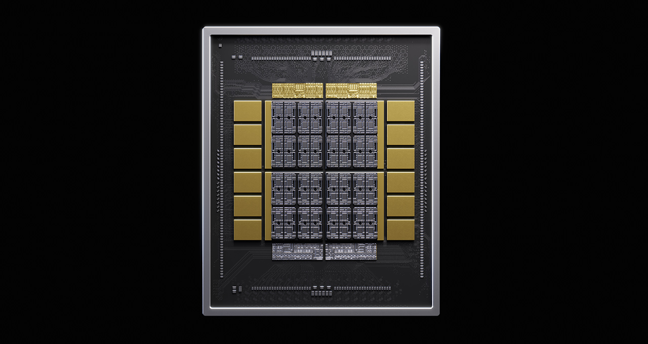
NVIDIA's real technical contribution here isn't just more GPUs - it's a redesign of how memory itself works. NVHBM relocates the memory controller out of the compute die entirely and moves it into the base die of the HBM memory stack itself, freeing up silicon area on the processor for more compute logic while increasing memory bandwidth and cutting power draw [1]. NVIDIA says the result is up to 30% more memory bandwidth, 15% lower HBM power consumption, and as much as 25% more usable compute-die area compared with standard HBM4E [1]. Amazon's chip-design unit, Annapurna Labs, is the first outside partner working with NVIDIA on this technology - notable because Annapurna is the same group that designs AWS's own Trainium processors.
That overlap is the tell. For Trainium4, this NVHBM work sits alongside NVLink Fusion, the interconnect technology AWS first flagged at re:Invent 2025 [2]. NVLink Fusion chiplets can connect up to 72 custom ASICs all-to-all at 3.6 TB/s per chip, adding up to 260 TB/s of total scale-up bandwidth through the Vera-Rubin NVLink switch tray [2], built on next-generation NVLink 6 running roughly 28 times faster than PCIe Gen5 [3]. In practice, AWS's own silicon and NVIDIA's GPUs are being wired into the same physical fabric, not kept as separate product lines competing for the same rack slot.