How AMD turned a chip into a frozen brain
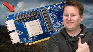
Taalas does not build a general-purpose processor and load a model onto it afterward. Its model-specific integrated circuits, or MSICs, etch a model's weights and dataflow directly into the transistors and metal layers of the chip itself, replacing the external high-bandwidth memory GPUs rely on with an on-die Mask-ROM fabric for weights and an SRAM fabric for KV-cache and fine-tuning adapters [1]. The company's HC1 test chip, an 815 square millimeter die built on TSMC's 6-nanometer process with 53 billion transistors, runs in a 2.5-kilowatt server configuration [2]and served Meta's Llama 3.1 8B model at close to 17,000 tokens per second, a speed Taalas said was 48 to 73 times the throughput of Nvidia's H200 and B200 GPUs at a fraction of the power draw [12]. Independent testing by analyst Karl Freund of Cambrian AI measured throughput at 14,357 tokens per second on the same chip, close to Taalas's own reported number [4]. The tradeoff is rigidity: once a chip is fabricated for one model, it cannot be reprogrammed for another. Taalas says updating to a new model only requires changing about two of the more than 100 metal layers on the die, cutting a full respin down to roughly a two-month tapeout rather than a from-scratch redesign [1], but every model swap still means new silicon, not a software update.