The Quiet Pivot: From Shrinking Transistors to Compressing Time
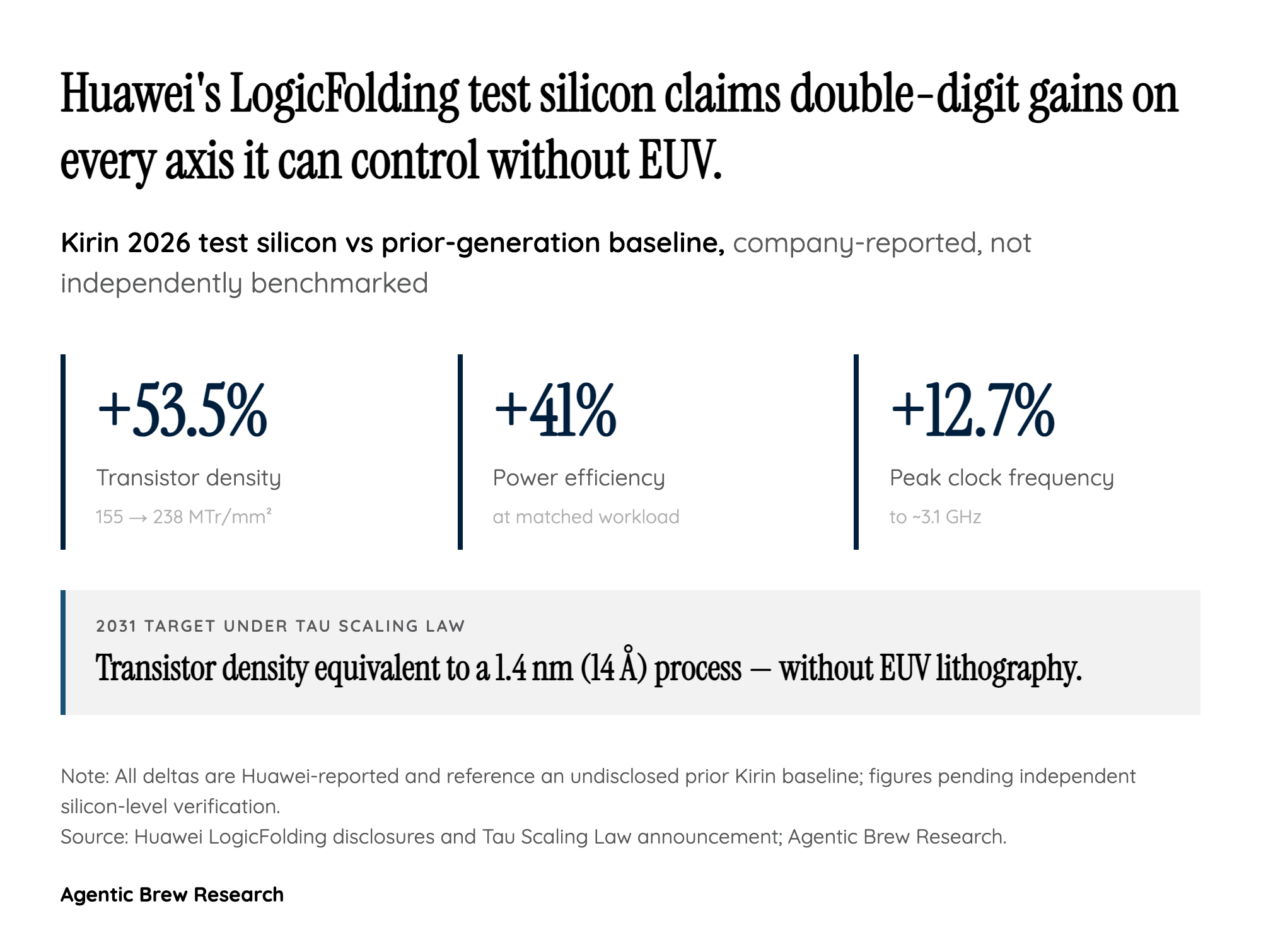
The intellectual core of Huawei's announcement is not a new transistor, it is a new objective function. The Tau (τ) Scaling Law re-anchors chip design around minimizing signal-propagation delay across every layer of the system rather than around shrinking gate length — a deliberate move away from geometric scaling as the main optimization target [1]. In practice that means three things working together: LogicFolding, which folds logic into a vertically stacked dual-layer architecture to shorten critical-path wiring; a UnifiedBus interconnect protocol that gives SuperPoDs unified memory addressing and lower communication latency [1]; and a co-optimization loop that treats device, circuit, chip, and system as a single search space.
The reframing matters because it changes how 'progress' is scored. Under Moore's Law, progress meant nanometers and transistor count; under Tau, progress means cycle time and end-to-end latency for a workload. If Huawei can hit a 14 Å (1.4 nm) transistor-density equivalence by 2031 without EUV, as the company claims [2], the bar for competitive silicon stops being 'which foundry can pattern the smallest gate' and becomes 'which design team can squeeze the most useful work out of a given lithography envelope.' For an industry that has spent fifteen years debating the death of Moore's Law, that is a coherent answer — even if Huawei is far from the only player working it.