The Sanctions Chess Move That Renamed the Goal
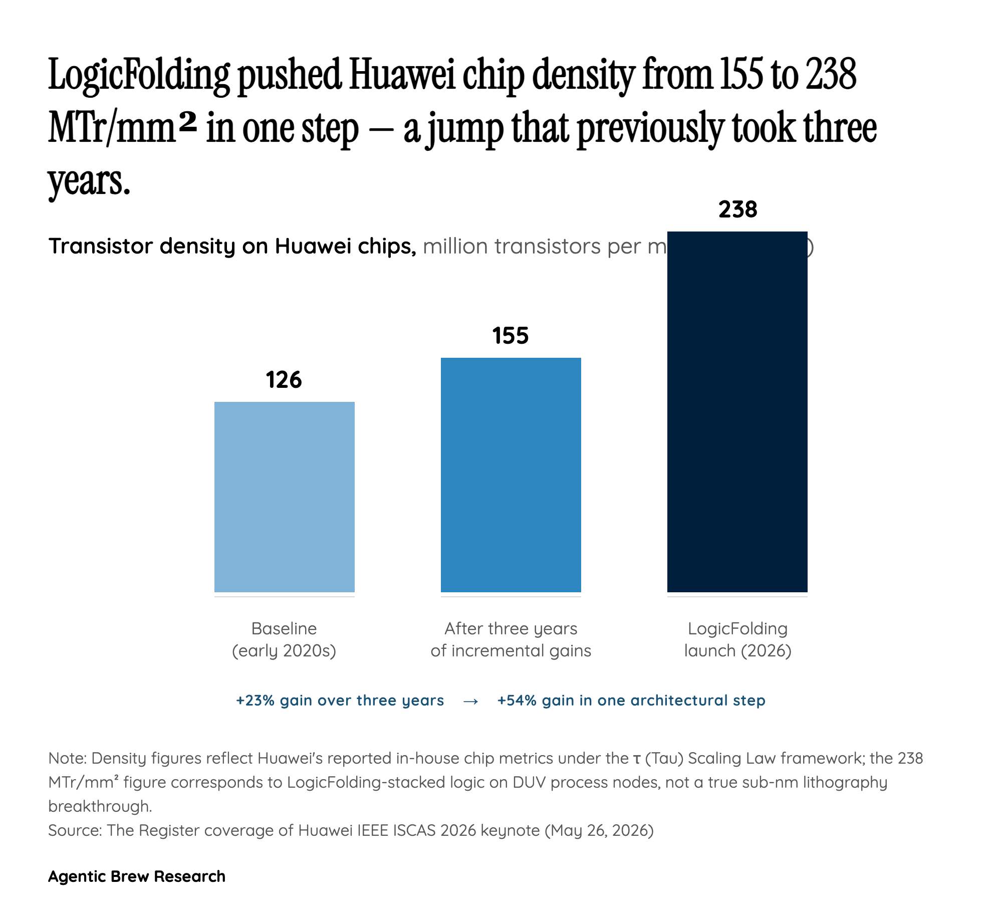
When Washington tightened export controls and ASML's EUV machines stopped flowing east, China's leading-edge chip ambitions ran into a single chokepoint: lithography. Without EUV, SMIC could not credibly chase TSMC's 3nm or 2nm node, and Huawei's Kirin and Ascend roadmaps were effectively pinned at a DUV-class 7nm process. The Tau Scaling Law, unveiled by Huawei semiconductor president He Tingbo at the IEEE ISCAS conference in Shanghai on May 25, 2026 [1], is the architectural reply — not an attempt to recover the chokepoint, but a move to make the chokepoint matter less.
The rhetorical move is the entire trick. Moore's Law was always a statement about feature size: every two years, you fit twice as many transistors in the same area. Tau, written as τ, is a time constant — the RC delay along which a signal actually propagates across silicon. By declaring that semiconductor progress should be measured in picosecond reductions of τ rather than nanometer reductions of pitch, Huawei is rewriting which competition it is in. On lithography, it loses; on signal-delay engineering across devices, circuits, chips, and systems, it claims to lead.
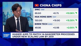
Markets and Chinese sell-side research read this signal accordingly. Bernstein called the announcement another DeepSeek-style milestone for China's tech stack [2], and CITIC Securities framed Tau as a methodology shift from chasing process linewidth to using system topology optimization to bridge short-term process gaps [2]. SCMP framed the keynote as Huawei's path to 14 Å-equivalent density by 2031 [3]. The story China is telling itself is no longer that it will catch ASML — it is that ASML is now solving the wrong problem.