The End of the General-Purpose AI Chip
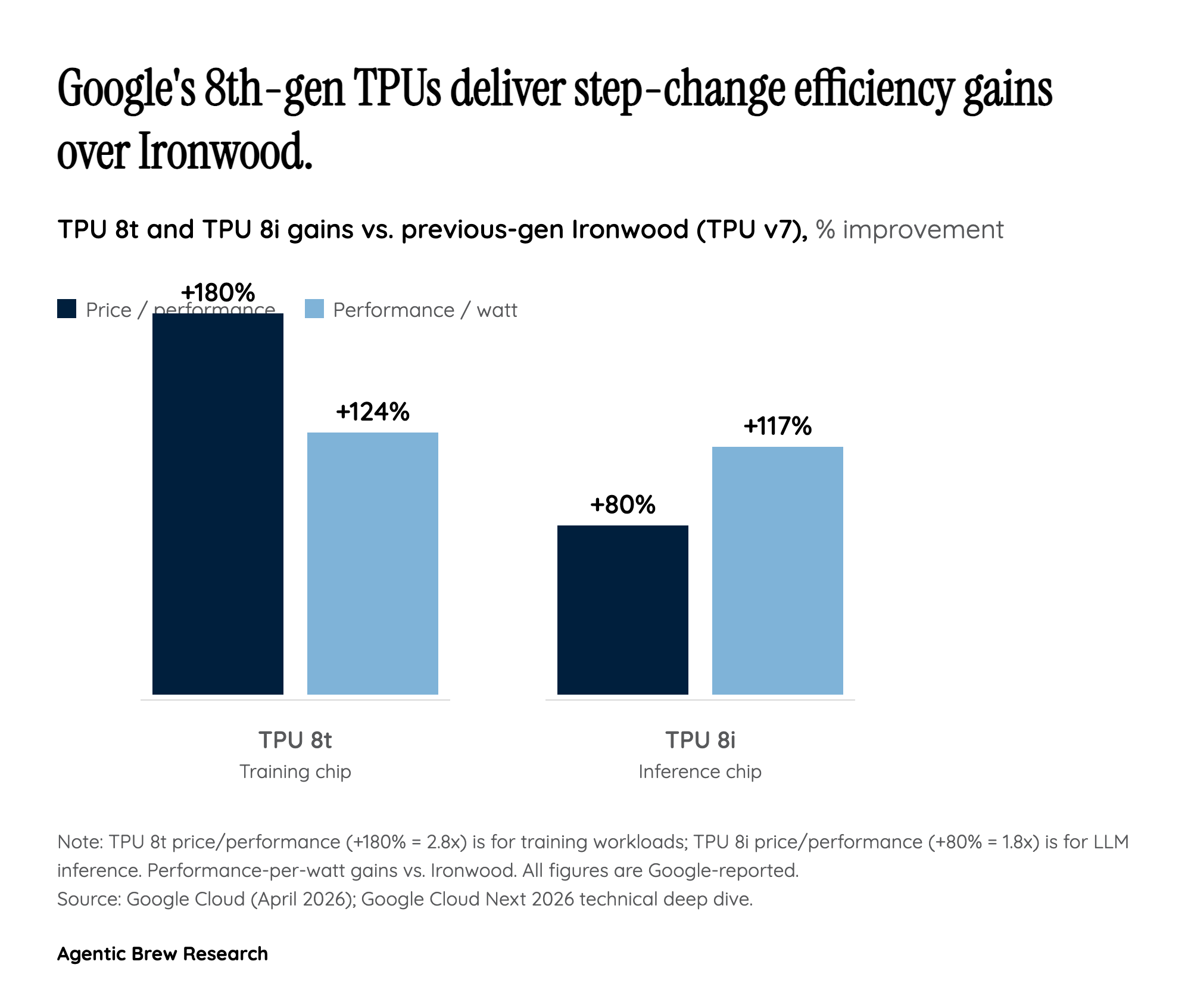
For twelve years, every TPU generation was a single part number trying to be good at both training and inference. TPU 8 ends that. Google split the line into TPU 8t, engineered to "reduce the frontier model development cycle from months to weeks," and TPU 8i, a serving chip "optimized for post-training and high-concurrency reasoning." The two chips share a fabrication lineage but diverge at the level that matters most: memory hierarchy and network topology.
TPU 8t is built around shared high-bandwidth memory at pod scale — 9,600 chips pooling two petabytes of HBM so that trillion-parameter training runs can treat the superpod as one logical accelerator. TPU 8i goes the other direction: Google packed it with "our highest on-chip SRAM, a new Collectives Acceleration Engine (CAE), and a new serving-optimized network topology called Boardfly." SRAM favors the short, bursty memory accesses of token generation; CAE accelerates the all-reduce operations that dominate multi-chip inference; Boardfly is tuned for many small, latency-sensitive serving groups rather than one giant training fabric. Hyperframe Research's read of this is blunt: the era of the general-purpose AI accelerator is over, and "specialized TPU 8t and 8i architectures signal the end of general-purpose silicon." That thesis, if right, reshapes how every hyperscaler plans its next chip.