The packaging revolution is the real headline, not 2nm
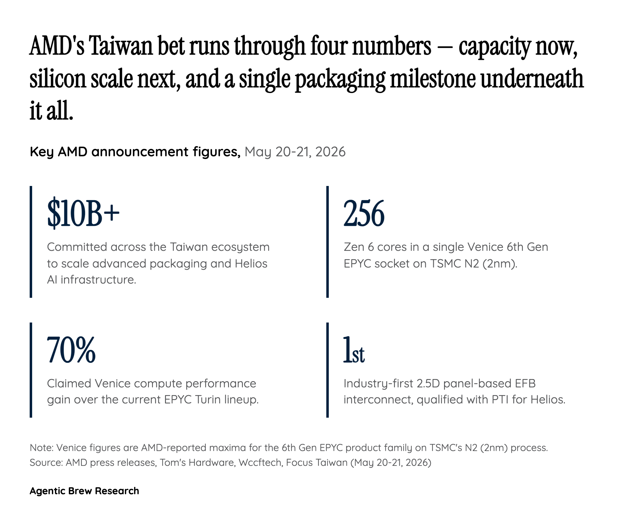
Most coverage led with 'first HPC chip on TSMC 2nm' [1], but the more consequential technical milestone is buried lower: AMD qualified the industry's first 2.5D panel-based Elevated Fanout Bridge (EFB) interconnect with PTI, and is co-developing a wafer-based EFB variant with ASE and SPIL [2]. Panel-based packaging is a structural break from wafer-based assembly — it moves advanced packaging onto larger rectangular substrates, dramatically improving area utilization and per-unit cost for the very large chiplet-plus-HBM stacks that AI accelerators need. This matters because the dirty secret of 2026 is that silicon is no longer the binding constraint. IndexBox analysts explicitly call advanced packaging 'one of the tightest constraints in the AI chip market right now' [3], and ASE's advanced packaging revenue is forecast to roughly double in 2026 [3]. By co-investing directly into EFB qualification with three different OSATs (Outsourced Semiconductor Assembly and Test providers), AMD is doing something less visible in Nvidia's playbook: treating packaging as a co-designed first-class component of the platform rather than an outsourced step. If Helios ships at multi-gigawatt scale in H2 2026 [4], it will be because EFB qualified — not because 2nm wafers showed up.