The math doesn't math: why $119B is the floor, not the ceiling
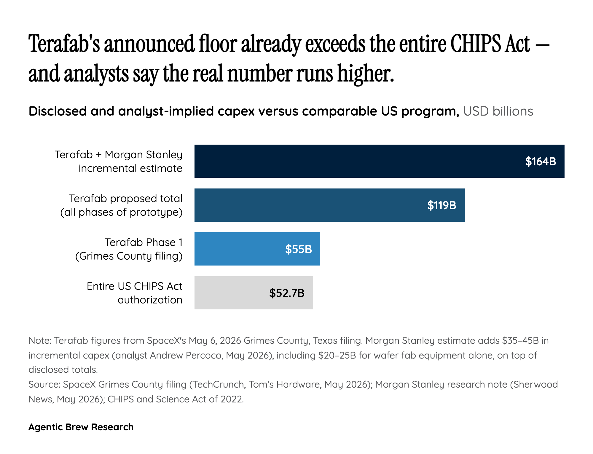
Start with the headline. SpaceX's Grimes County filing pegs Terafab's prototype phase at $55B initial, scaling to $119B. That floor alone already exceeds the roughly $52.7B Congress authorized through the entire CHIPS Act for the U.S. semiconductor industry. It is the largest single semiconductor capex commitment ever proposed in this country, and it is supposedly only the first phase. Then look at what Terafab is meant to do: more than one terawatt of AI compute per year, ramping from 100,000 wafer starts per month toward a million. A million wafer starts monthly is roughly 12 million wafers a year, at the same order of magnitude as TSMC's entire advanced-node output today.
Morgan Stanley's Andrew Percoco, who is broadly positive on the strategy, still adds $35-45B on top of the disclosed numbers — $20-25B of that is wafer fabrication equipment alone, none of which lives inside Tesla's $20B/yr existing capex budget. Tesla has not raised, segregated, or even acknowledged the marginal capital. The hard physical bottleneck the announcement skipped past entirely is ASML: there are roughly 40-55 EUV lithography machines built globally per year, and a single fab at Terafab's claimed scale would consume a meaningful fraction of worldwide EUV supply for years. That is the pivot behind the technical estimates circulating in semiconductor-literate forums — extrapolating Musk's own 1 TW/year capacity claim against his $200B framing yields an implied total program cost closer to $5 trillion. The skeptics are not arguing about ambition. They are arguing about arithmetic — announced numbers, EUV machine counts, and wafer-throughput physics that do not reconcile.